
Many low cost SDR platforms are now available on the market, such as HackRF One [1], Adalm Pluto [2], and the USRP product line [3], to name only a few. What these platforms have in common is that the baseband processing is carried out in a field-programmable gate array (FPGA). Another common characteristic is the instantaneous bandwidth, which is typically 20 MHz.
In this project we propose a large-bandwidth low-cost SDR architecture based on a Red Pitaya board. The components of this architecture are chosen so that the bottleneck in the transmit/receive chain will be the board.
RF transceiver architecture
The proposed transceiver architecture is presented in Figure 1, which can be understood as a Zero-IF transceiver. The Red Pitaya board comprises the baseband processor in the FPGA and the Analog/Digital conversion stages. The RF output bandwidth of the RED Pitaya is approximately 40 MHz, but the onboard ADC supports 125Msps. The I/Q modulator stage is carried out with a demo board 2391A [4] that is optimized for evaluation of the LTC5589 low-power I/Q modulator up to 4.5GHz. The four balanced I- and Q-baseband input ports can be either AC-coupled with internal bias supplied, or DC-coupled from a source with a common-mode voltage level of about +1.4V. The SPI interface is used to set internal registers which control the gain, optimum center frequency, I-offset, Q-offset and sideband suppression. In addition to the digital gain control with 1dB steps, there is an analog gain control, VCTRL. An on‑chip thermometer can be used to compensate for the gain vs temperature variations using a digital gain control change. The update can either be automatically triggered, or entirely switched off.
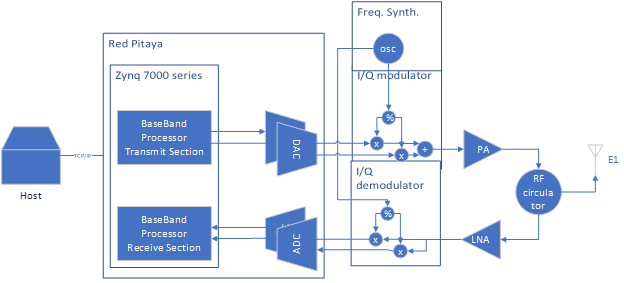
Figure 1: High-bandwidth low-cost SDR platform
The power amplifier (PA) stage could be carried out with a low-cost TRF37x75 EVM [5] dev-board. The Texas Instruments TRF37x73 RF Gain Block Amplifiers are packaged in a 2.00mm × 2.00mm WSON with a power down pin feature making them ideal for applications where space and low power modes are critical. The TRF37x73 is designed for ease of use. For maximum flexibility, this family of parts uses a common 3.3V supply and consumes 52mA (TRF37B73), 53mA (TRF37D73) or 55mA (TRF37A73, TRF37C73). In addition, this family was designed with an active bias circuit that provides a stable and predictable bias current over process, temperature, and voltage variations. For gain and linearity budgets, the device was designed to provide a flat gain response and excellent OIP3 out to 6000 MHz. For space constrained applications, this family is internally matched to 50Ω, which simplifies the ease of use and minimizes the PCB area needed.
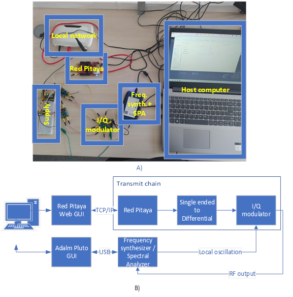
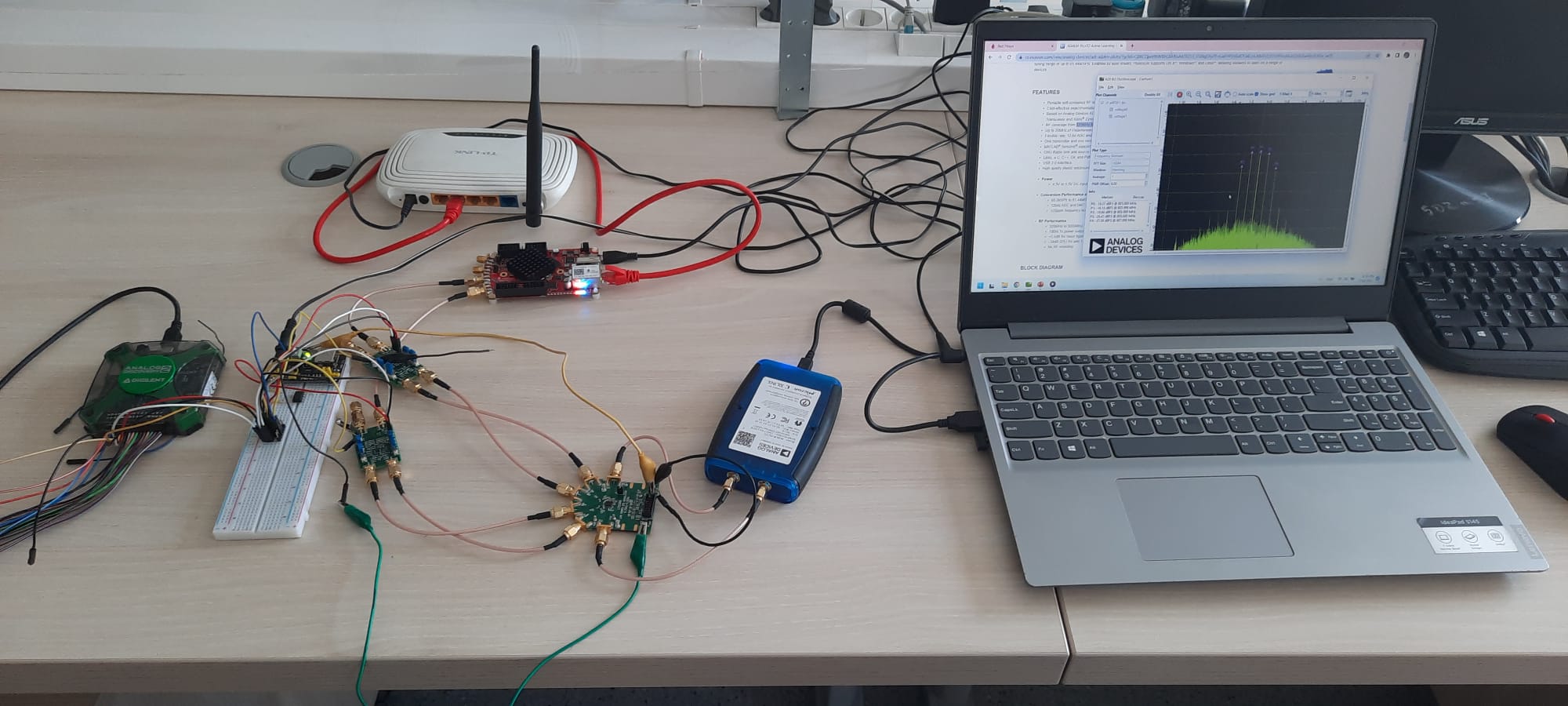
Figure 2: Setup for transmit chain testing: a) actual setup, b) conceptual illustration
The modulator stage is also fed by the carrier signal, generated by a low-cost MAX2870 23.5-6000 MHz RF Signal Source Signal Generator Module PLL VCO w/ STM32 [6] development board. This board features an ultra-wideband phase locked loop (PLL) and an integrated voltage-controlled oscillator (VCO), able to generate a 23.5 MHz to 6.0GHz frequency range signal output. The board can maintain excellent phase noise and spurious indicators, and it provides dual-channel differential output drivers, which can be individually set to provide output power from -4 dBm to +5 dBm.
The demodulator stage is carried out by an LTC5586 demo board [7] circuit, and the 2349A’s two switchable single-ended RF inputs are optimized for 700 MHz to 6GHz. Its single-ended LO input is programmable for 300 MHz to 6GHz operation via SPI bus. The demo circuit includes discrete L-C inter-stage lowpass filters between the demodulator outputs and the IF amplifier inputs, which limits the DC-coupled differential I and Q outputs to about 500 MHz (–1dB bandwidth).
The receive side of the transceiver is solved with the Red Pitaya board and it’s RF input section. The nominal bandwidth of the ADC is 50 MHz, but the sampling rate is 125Msps.
Experimental results
A portion of the transmit chain was carried out and tested using the setup presented in Figure 2. A local network is created with the use of a router. The Red Pitaya development board and host computer are connected to this local network. As the host computer and Red Pitaya dev-board are in the same network, the web interface of the dev-board is accessed from a browser run on the host computer. An Adalm Pluto device is used to generate a local oscillation and inspect the RF signal generated by the transmitter chain.
The next test cases were as follows: 1. A carrier tone is generated. 2. A double-sideband modulation of a 1 MHz sine wave is generated. 2. A double-sideband modulation of a 2-tone signal is generated.
- Carrier generation. First, a local oscillation of 805 MHz is generated by the Adalm Pluto. The spectrum analyzer plots the spectrum of the carrier, as shown in Figure 3. The center frequency of the spectrum analyzer is set to 800 MHz. A carrier of 10 dBm can be clearly seen at 805 MHz.
- A 1 MHz tone is generated for the in-phase component of the I/Q modulator. For this purpose, the Red Pitaya web GUI was used, namely the Arbitrary Signal Generation section. The setup is presented in Figure 4 a.
- A 2-tone is generated for the in-phase and quadrature components of the I/Q modulator, one tone is at 1 MHz, the second ton is 2 MHz. For this purpose, the Arbitrary Signal Generation section of the Red Pitaya web GUI was used again. The setup is presented in Figure 4b.
The results of the double-side modulation for cases 2 and 3 are presented in Figures 5 and 6, respectively. The spectrum analyzer is centered at 800 MHz, and thus the carrier at 805 MHz is 10 dBm. Figure 5 shows the double-sideband modulation, and it can be seen that at the 1 MHz sine wave the modulator signal causes two peaks, at 804 an 806 MHz. In Figure 6, beside the carrier at 805 MHz, 4 spectral components are present at 803, 804, 806 and 807 MHz.
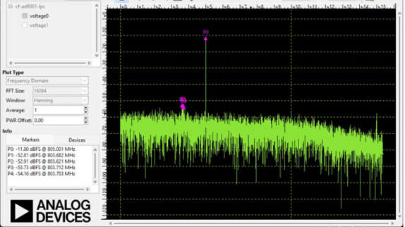
Figure 3: The 800 MHz carrier generated by the Adalm Pluto
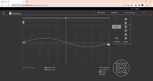
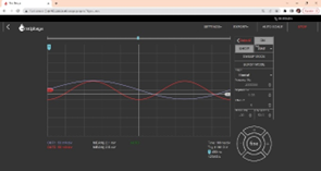
Figure 4: Red Pitaya Web GUI to setup a) a 1-tone sine wave, b) a 2-tone signal.
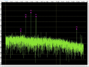 Figure 5: Double-sideband modulation of a 1 MHz sine wave
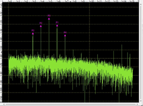 Figure 6: Double-sideband modulation of a 2-tone signal
In this project a novel large-bandwidth low-cost SDR architecture is proposed. The proposed SDR is a zero IF transceiver, where the Red Pitaya board is used for baseband processing. The bandwidth of the RF input and output is 50 MHz, but the board allows for higher sample rates. A portion of the transmit chain was implemented in an experimental setup, and the transmit chain was demonstrated using 3 test cases: 1. a carrier is generated; 2. a 1-tone signal is double-sideband modulated; 3. a 2-tone signal is double-sideband modulated.
References
[1] https://greatscottgadgets.com/hackrf/
[2] https://ro.mouser.com/datasheet/2/609/ADALM-PLUTO-Product-Highlight-1633770.pdf
[3] https://www.ni.com/pdf/product-flyers/usrp-software-defined-radio.pdf
[4] Linear Technology Corporation, DEMO MANUAL DC2391A - 700 MHz to 6000 MHz LOW POWER I/Q MODULATOR, 1630 McCarthy Blvd., Milpitas, CA 95035-7417
[5] Texas Instruments, “TRF37x73 and TRF37x75 EVMSLAU546A User’s Guide”, March 2014, Revised October 2021
[6] Maxim Integrated, “23.5 MHz to 6000 MHz Fractional/Integer-N Synthesizer/VCO”, 19-6250; Rev 6; 4/17
[7] Linear Technology Corporation, “DEMO MANUAL DC2349A - LTC5586 6GHz High Linearity I/Q Demodulator with Wideband IF Amplifier”, 1630 McCarthy Blvd., Milpitas, CA 95035-7417


