
Explore the world of FPGA design with this comprehensive guide focused on using Simulink and CASPER, specifically tailored for the Red Pitaya platform. This guide simplifies the process of setting up your design environment, utilizing essential libraries, and configuring your project for success. Start with a basic flashing LED project to grasp FPGA design principles and practical application. Our guide also covers the critical steps of software interaction, simulation to validate functionality, and the transition from simulation to hardware through compiling and programming. This journey from concept to real-world application equips you with the foundational skills needed for advanced FPGA projects, enabling you to unlock the full potential of FPGA technology.
Setting Up Your Design Environment
Beginning with FPGA design requires precise setup of your development tools. This involves launching MATLAB, starting Simulink from the command prompt, and creating a new project. It's essential to choose meaningful project names without spaces or capital letters, and to save your work regularly to avoid data loss and ensure toolchain compatibility.
Utilizing Libraries for FPGA Design
Simulink and CASPER offer comprehensive libraries for FPGA development:
- CASPER XPS Library: Houses Yellow Blocks for easy interfacing with hardware like ADCs and DACs, streamlining the design process.
- CASPER DSP Library: Contains blocks for digital signal processing tasks, optimizing your design for high-performance computations.
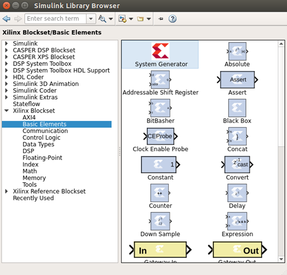
- Xilinx Library: Provides fundamental blocks for FPGA development, including the critical System Generator block that outlines your target FPGA device.

These libraries enable you to craft advanced FPGA designs by providing a high-level approach that abstracts the complexities of hardware programming.
Configuring Your Project
Proper initial configuration is key to a successful FPGA project:
- System Generator Block: Place this block from the “Xilinx library” into your model to specify your FPGA target. This block acts as a pivotal reference throughout the design process.
- Platform Block Selection: From the “CASPER library”, add a platform block corresponding to your hardware, like a Red Pitaya device. This block tailors the System Generator settings to your specific FPGA, including clock sources and pin configurations, ensuring hardware compatibility.
These steps form the foundation of your FPGA design, effectively linking your Simulink model with the physical FPGA board's capabilities.
Flashing LED: Your First Hardware Interface
When starting with FPGA design, a flashing LED circuit is the ideal first project. It serves as both an introduction to FPGA design principles and a practical verification of your setup:
- The core of our flashing LED circuit is a counter. We will use a 27-bit free-running counter from the Xilinx library. This counter increments continuously from 0 to .
- Given a clock frequency (Red Pitaya Clock Speed) of 125 MHz, the counter toggles the MSB roughly every 0.67 seconds.
- Extracting the MSB: To achieve the flashing effect, we focus on the most significant bit (MSB) of the counter. Extracted using a slice block, this MSB alternates states at a frequency ideal for our purposes—driving an LED to flash.
- Connecting to the LED: The final step is linking the MSB to an FPGA board LED via a GPIO block from the CASPER library. This process vividly demonstrates how digital signals can directly influence physical hardware components, in this case, causing the LED to blink.

Beyond the Basics
After mastering the flashing LED project, the guide progresses to cover more complex concepts, such as building an adder circuit. This section introduces the reader to the FPGA's computational capabilities, illustrating basic arithmetic processing and further expanding your FPGA design skills. This approach not only solidifies your understanding of FPGA basics, but also prepares you for more advanced topics and projects, like the adder circuit mentioned above, ensuring a well-rounded entry into the world of FPGA design. The guide for designing the adder can be found here.
Software Interaction
The ability to interact with your FPGA design through software not only enhances its flexibility, but also its applicability to real-world scenarios. By integrating software registers into your design, you enable dynamic control and monitoring capabilities from a computer.
- Adding Software Registers: Software registers are interfaces that allow software applications to read from and write to specific locations in your FPGA's memory, effectively controlling or monitoring aspects of the FPGA's operation. Add two types of registers to your design: one for control (to start, stop, and reset the counter) and another to read its current value. This setup exemplifies how software can influence hardware behavior and retrieve data from it.
- Implementing Control Logic: With the registers in place, the next step is to incorporate logic into your design that responds to the software commands. This involves setting up conditions within your FPGA design that check the register values, and then based on these values, control the counter's operation. For example, you could implement a logic block that resets the counter when a certain value is written to the control register.

This approach not only demonstrates the fundamental principle of software-hardware interaction, but also lays the groundwork for more complex control schemes in advanced projects.
Simulating Your Design
Simulation is a pivotal step in the FPGA design process with Simulink, offering a powerful tool to validate your design's functionality, performance, and reliability without the immediate need for physical hardware. To simulate your design, simply follow these steps:
- Setup: Configure your Simulink model to reflect your FPGA's operational parameters, including a fixed-step solver and accurate simulation timing to mimic real-world behavior.
- Execution: Run the simulation via Simulink's play button, observing key outcomes like LED toggling to validate the expected behavior.
- Analysis: Use Simulink's visualization tools to examine your design, identifying areas for optimization to ensure your project meets its goals.

Simulation in Simulink is essential for ensuring your FPGA design works as intended before moving to hardware. Set up your model to reflect the FPGA's conditions, including timing and operations. Running the simulation brings your design to life, allowing you to observe and verify functionality, like the flashing LED's behavior. Analyzing these results with Simulink's tools helps pinpoint and correct issues, optimizing your design for real-world application. This crucial step paves the way for efficient and successful hardware implementation.
From Simulation to Hardware: Compiling and Programming
After a successful simulation, moving your design to an FPGA involves:
- Compilation: Use the “jasper” command in MATLAB to start converting your Simulink model into an FPGA-compatible bitstream, incorporating synthesis, placement, and routing. This step, which is dependent on your design's complexity, prepares your project for actual deployment.
- Programming: With the generated bitstream, employ the “casperfpga" Python library to program your FPGA. This involves connecting your computer to the FPGA board and transferring the bitstream file, setting the stage for real-world operation.
- Verification: Finally, check your FPGA board to confirm the design works as simulated, such as seeing the LED flash in sync with your model. This validation step bridges your work from concept to reality, showcasing the effectiveness of your FPGA design.
After refining your design through simulation, compiling it into an FPGA-compatible format is next. Use MATLAB's "jasper” command to initiate this process, transforming your Simulink model into a bitstream file that FPGAs can understand. This step, involving synthesis and routing, prepares your design for the real world. Following compilation, program your FPGA using the “casperfpga” Python library, uploading the bitstream to your board. Successfully programming and verifying your design on the FPGA board confirms the transition from a simulated model to a tangible, functioning system, showcasing the power and versatility of FPGA technology.
Conclusion
This tutorial has provided a comprehensive overview of FPGA design using Simulink and the CASPER framework. From conceptualizing a simple hardware interface to implementing arithmetic processing and enhancing the design with software interaction, you have learned the essentials of FPGA design. Simulation plays a crucial role in this process, serving as a bridge between design and real-world implementation, ensuring that your projects are not only imaginative but also viable and robust.
Armed with these foundational skills, you are now well-prepared to explore more advanced designs, pushing the boundaries of what is possible with FPGA technology.
Want more?
- CASPER documentation
- Red Pitaya CASPER tutorials


