Modern high-speed optical systems—such as hyperspectral imaging, interferometry, and spectroscopy—generate data faster than traditional centralized servers can process, creating massive bandwidth and storage bottlenecks. Shifting from centralized cloud architectures to on-device edge processing (using SoCs and FPGAs) solves these challenges by computing data at the measurement source, enabling real-time feedback, reduced network overhead, and enhanced data security.
What is Edge Processing in Optical Measurement?
Edge processing performs computational analysis directly at or near the sensor source rather than transmitting raw data streams across networks to remote servers or cloud platforms.
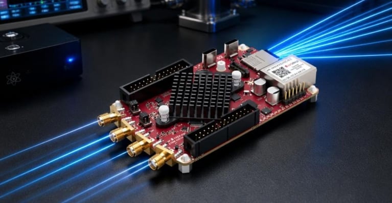
By analyzing high-resolution optical data locally, edge hardware—such as Field Programmable Gate Arrays (FPGAs) and System-on-Chip (SoC) platforms like Red Pitaya STEMlab—extracts key metrics instantaneously and transmits only the processed results (e.g., pass/fail decisions or spectral features) back to the network.
Key Takeaways: Centralized vs. Edge Processing
| Feature |
Centralized / Cloud Processing |
Edge Processing (Red Pitaya SoC/FPGA) |
| Response Latency |
Seconds to hours (Network transfer & queueing) |
Sub-millisecond to real-time closed loops |
| Bandwidth Demand |
Massive (Streams gigabytes of raw sensor data) |
Minimal (Transmits only extracted features/metrics) |
| Data Security |
High risk (Sensitive raw data sent over network) |
Enhanced (Raw measurement data never leaves local hardware) |
| System Resilience |
Fails during network outages |
Autonomous (Continues operating offline) |
| Operational Cost |
High (Continuous cloud storage & network upgrades) |
Lower TCO (One-time hardware deployment, low bandwidth) |
4 Core Benefits of Edge Computing for Photonics
- Sub-Millisecond Feedback Loops: Moving processing directly onto the hardware enables closed-loop control. Vision and inspection systems can detect surface defects or spectral anomalies instantly, halting production lines or adjusting laser parameters in real time.
- Exponential Bandwidth Reduction: Instead of transmitting gigabytes of raw video or waveform streams, edge algorithms compress and filter the data locally, sending only clean, calibrated metrics (reducing data payload from gigabytes to kilobytes).
- Improved Reliability & Compliance: Industrial and research setups remain operational during network interruptions. Keeping raw measurement data on local hardware simplifies compliance and protects proprietary intellectual property.
- Accessible, Compact Hardware: Modern SoC and FPGA boards bring high-performance computing to budget-conscious R&D labs without requiring massive server infrastructure.
Real-World Photonics Applications
- Machine Vision & Defect Inspection: High-speed line inspection for pharmaceutical and semiconductor manufacturing that verifies quality unit-by-unit at full production speeds.
- On-the-Fly Spectroscopy: Chemical signature detection that flags compositions of interest mid-experiment without waiting for offline post-processing.
- Surface Interferometry: Real-time generation of nanometer-precision surface topology maps during component production.
- Biomedical OCT & Ultrasound: Immediate image reconstruction allowing real-time adjustment of scanning parameters during clinical or lab acquisitions.
Read the Full Published Article
To dive deeper into the hardware architectures, cost analyses, and technical implementation strategies of edge processing in optical test systems, read the full article on Vision Systems Design.
Technical FAQ for Optical Instrumentation & Vision Engineers
How does edge processing eliminate data bottlenecks in high-speed optical systems?
In high-speed optical applications like hyperspectral imaging, interferometry, or machine vision, instruments generate raw data faster than standard network pipelines and centralized servers can ingest it. Edge processing shifts computing power directly onto the sensor hardware (via SoCs or FPGAs like the Red Pitaya STEMlab). By running feature extraction, filtering, and pass/fail algorithms locally, the system transmits only refined metrics or decisions (reducing gigabytes of raw data down to kilobytes) rather than flooding the network infrastructure.
What is the latency advantage of edge platforms compared to cloud or centralized processing?
Centralized processing introduces inevitable transmission delays, queueing overhead, and network jitter—stretching feedback loops from seconds to hours. Edge processing architectures execute computations directly at the measurement source, delivering real-time, closed-loop feedback within milliseconds. This allows automated vision systems to halt production lines, reject defective components, or adjust laser scanning parameters mid-acquisition without human or cloud intervention.
How does edge processing improve data security and operational resilience in research environments?
Transmitting unencrypted, proprietary measurement streams across external or cloud networks creates security vulnerabilities and compliance challenges. Edge computing keeps raw, high-resolution datasets confined strictly within the local hardware environment, transmitting only anonymized or extracted numerical metrics across the network. Furthermore, because analysis occurs at the device level, optical inspection systems operate continuously and autonomously during network or internet outages, preventing costly manufacturing downtime.
Can budget-conscious laboratories implement edge processing without rebuilding their entire software stack?
Yes. Modern open-architecture System-on-Chip (SoC) platforms like Red Pitaya offer flexible FPGA environments, multi-core ARM processors, and support for standard programming languages (C, C++, Python) and APIs. Research teams can easily port existing optical signal processing and machine vision algorithms to edge hardware, bypassing the high total cost of ownership associated with enterprise cloud infrastructure, continuous bandwidth upgrades, and proprietary benchtop processing units.

 September 22, 2026