


Connecting Embedded Software Abstractions, Physical Bus Signals, and Connected BLE Systems with EESTEC LC Ljubljana
In embedded systems development, serial console logging via printk or Segger RTT is typically one of the first diagnostic tools an engineer reaches for, but software terminal output cannot reveal what occurs across physical circuit traces. Print routines add execution overhead and can affect the timing and scheduling behavior under evaluation. When transitioning from bare-metal super-loops to a preemptive Real-Time Operating System (RTOS), additional software abstraction layers are introduced. An application driver may compile cleanly and report a successful status code while the underlying peripheral bus suffers from marginal signal transitions, bus contention, or missing acknowledgments (NACKs).
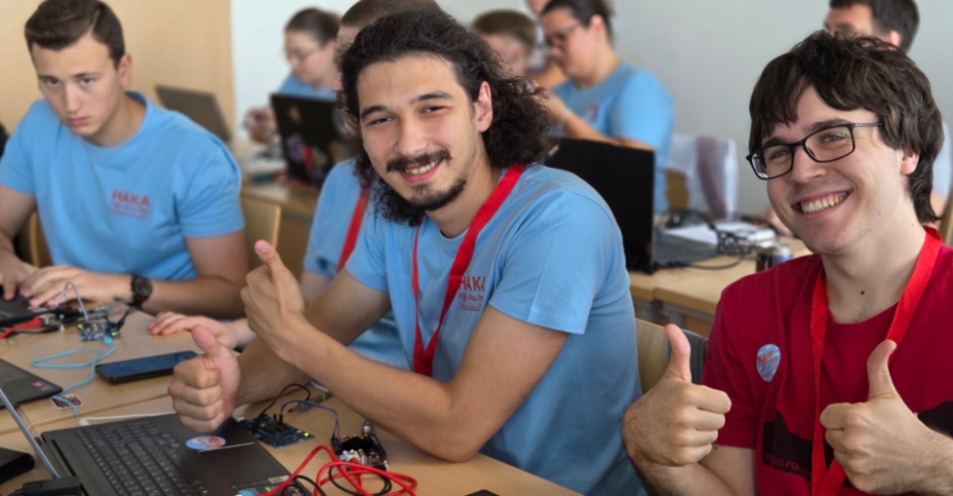
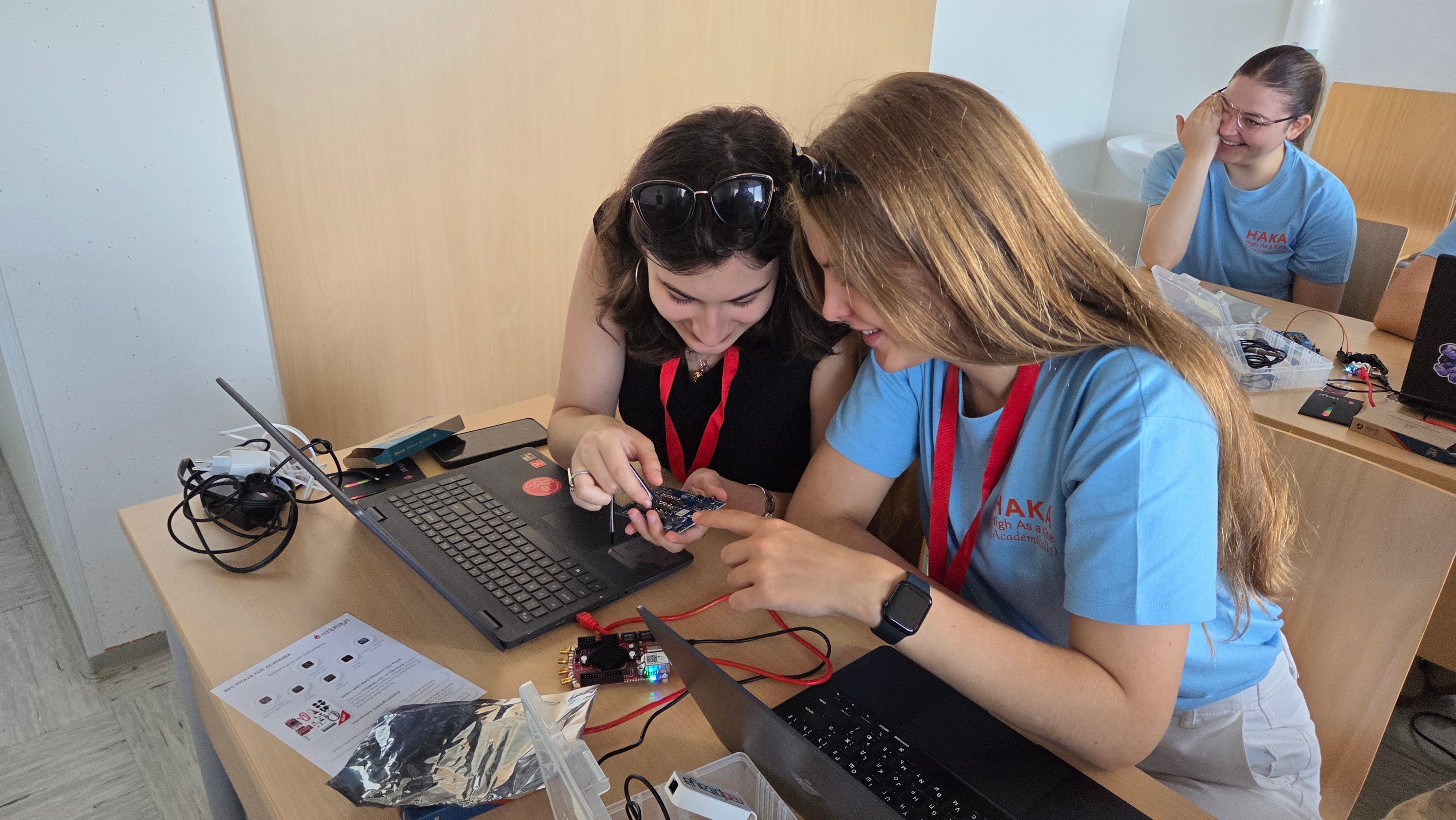
To examine how real-time firmware interacts with physical digital buses, 24 electrical engineering and computer science students gathered at the University of Ljubljana’s Faculty of Electrical Engineering for a five-day hands-on workshop organized by EESTEC LC Ljubljana. Supported by Red Pitaya and Nordic Semiconductor, the curriculum guided participants from multi-threaded RTOS fundamentals to physical protocol decoding and wireless system deployment.
Key Takeaways
- Exposing Physical Bus Errors: Software status codes can mask physical bus failures; the STEMlab 125-14 Logic Analyzer allowed students to visually decode I2C traffic and link driver errors directly to physical NACKs.
- Direct 3.3V FPGA Probing: Direct jumper connections between the Nordic nRF54L15 board and STEMlab’s Extension Header E1 enabled 3.3V LVCMOS signal capture on the Zynq-7010 FPGA without level shifters.
- Zephyr RTOS & Determinism: Participants built structured, real-time firmware using Zephyr RTOS, using Devicetree and Kconfig to control driver compilation and task priorities over bare-metal super-loops.
- Full-Stack BLE & FOTA: Students implemented custom GATT services, programmed central/peripheral roles, and integrated MCUboot to perform wireless Firmware Over-The-Air updates from smartphones.
- Extensible Bench Testing: The Red Pitaya platform enables future lab modules for Python-scripted automated long-term bus testing and oscilloscope-based signal integrity/RF coupling analysis.
The Hardware Setup: Bridging the Target MCU to the Logic Analyzer
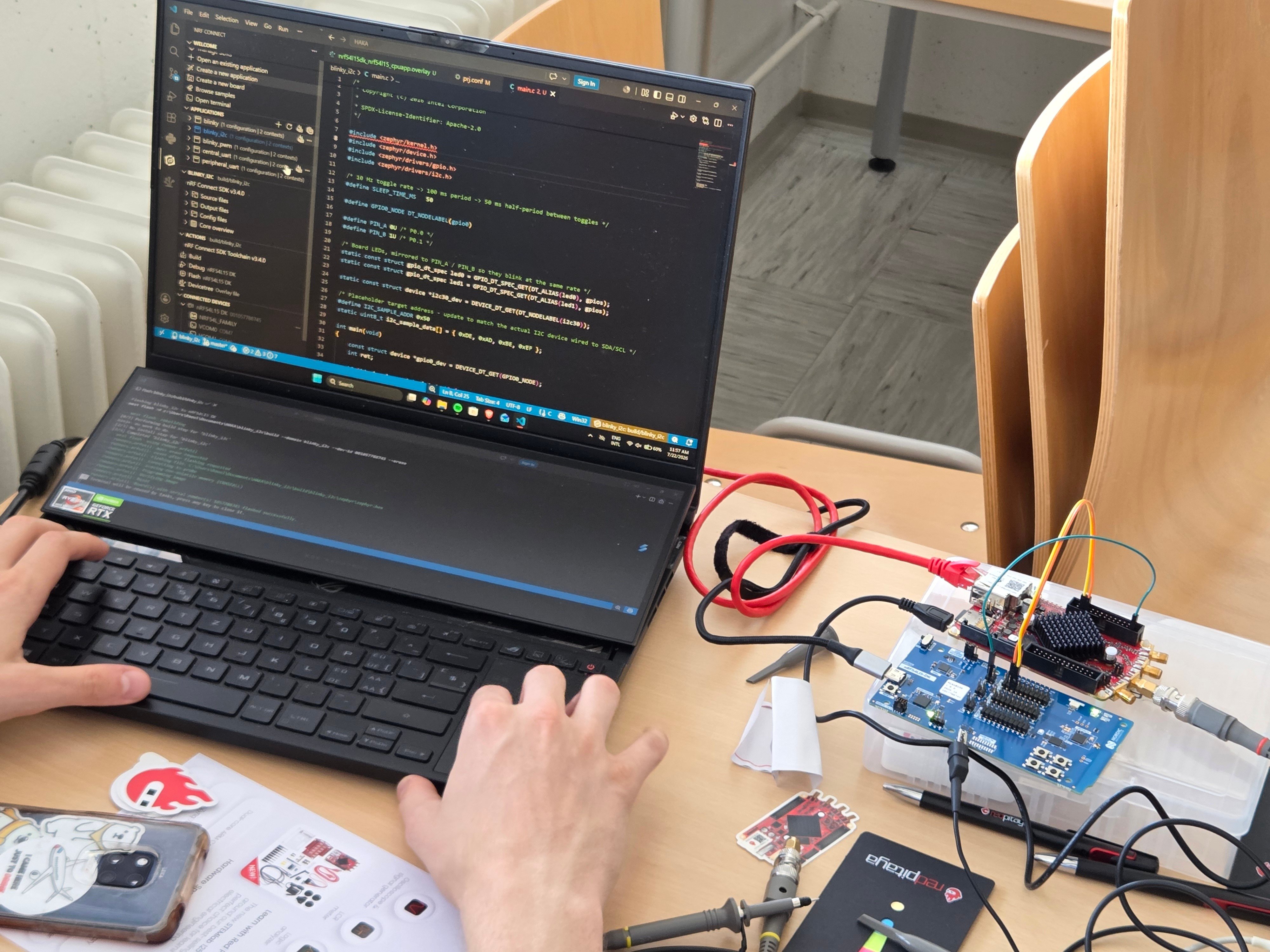
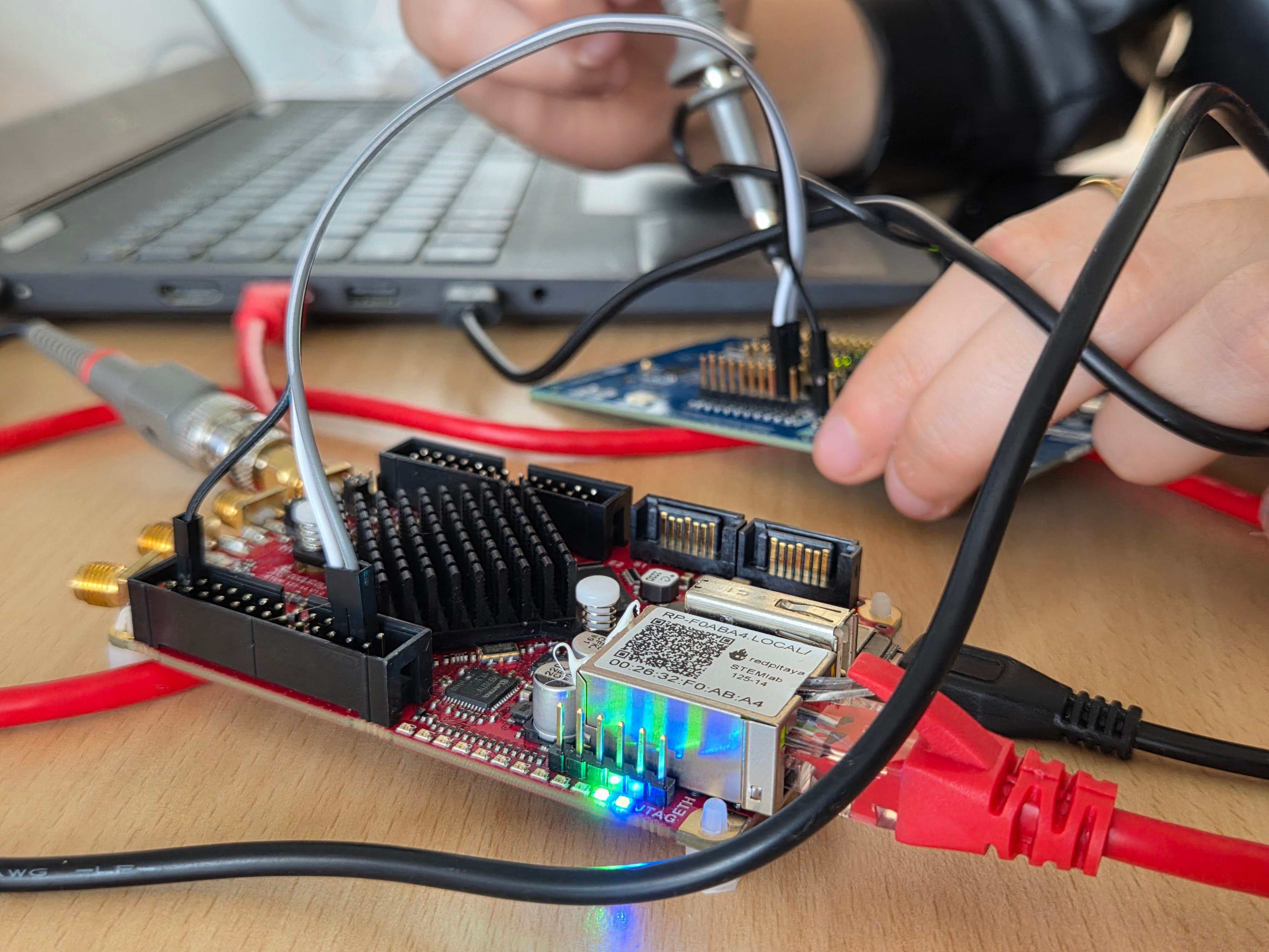
Rather than relying purely on software debuggers, each student workstation paired a Nordic Semiconductor nRF54L15 Development Kit (DK) with a Red Pitaya STEMlab 125-14 running its web-based Logic Analyzer application.
Direct jumper wires connected digital I/O lines (pins P0.01 and P0.02) from the Nordic board directly to Digital Extension Header E1 (DIO0_P and DIO1_P) on the STEMlab, establishing a shared reference to ground. Because the STEMlab’s digital header connects directly to the on-board Zynq-7010 FPGA pins configured for 3.3 V LVCMOS operation, the logic levels of the Nordic development kit were directly compatible with the STEMlab digital inputs, requiring no external level-shifting circuitry. This allowed the digital communication lines to be monitored directly while keeping signal voltages safely within the maximum input ratings of the FPGA bank.
The Curriculum & Signal Flow
1. Establishing Determinism with Zephyr RTOS
The workshop opened by evaluating bare-metal architecture, demonstrating how traditional polling super-loops and sprawling interrupt service routines struggle with concurrency as system requirements expand. Students restructured these tasks within Zephyr RTOS, establishing preemptive thread priorities and coordinating execution using semaphores and message queues. Working within the nRF Connect SDK, participants modeled peripheral nodes using Devicetree overlays (.overlay) while controlling driver compilation and kernel features through Kconfig files (prj.conf).
2. Physical Bus Verification with the Red Pitaya Logic Analyzer
Once peripheral drivers were running on the Nordic board, participants turned to the STEMlab 125-14 to observe physical line activity. Students could then follow the complete path from configuration to hardware: a Devicetree node enabled and mapped the peripheral, Kconfig brought the required subsystem into the build, Zephyr's driver API initiated the transaction, and the Red Pitaya Logic Analyzer revealed what actually appeared on the bus
Students first generated pulse-width modulated (PWM) waveforms on the Nordic board, observing duty-cycle consistency and period stability on the logic analyzer. The capture gave students a direct view of the generated waveform, connecting the firmware configuration on the Nordic board with the timing characteristics visible on the physical signal.
Next, students configured an I2C controller in Zephyr to inspect two-wire bus traffic. To simplify benchtop wiring and eliminate external breadboarding, the Nordic board’s internal pull-up resistors were enabled directly in the pin-control configuration.
Without an external sensor attached to the bus, executing an outbound driver call (i2c_write_read_dt()) created a practical protocol debugging scenario: the Red Pitaya Logic Analyzer decoded the transmitted 7-bit target address and clock stream, clearly displaying the missing acknowledgment (NACK) on the ninth clock cycle when no peripheral responded. This visual confirmation showed participants why the driver call returned an error code, connecting software return values directly to physical bus states.
3. Connected Peripherals and Over-the-Air Updates
With the physical interfaces confirmed, the focus turned to Bluetooth Low Energy (BLE). Students first implemented the Nordic UART Service (NUS) in a peripheral role, creating custom GATT characteristics to send commands and stream data to a mobile phone running the nRF Connect application. The students then flipped roles, programming the target board as a BLE central device to scan, connect, and log data from external sensor nodes.
Because the group completed the core driver milestones ahead of schedule, the curriculum moved beyond the planned flash-storage exercises and tackled Firmware Over-The-Air (FOTA) updates. Under the guidance of EESTEC instructor Bor, students integrated the MCUboot bootloader into their Zephyr projects, generated update .zip archives, and performed firmware updates wirelessly over BLE using their smartphones—verifying operational firmware swaps in the field without attaching a debug probe.
Expanding the Bench: Automated Testing and Signal Integrity
Looking beyond the workshop, Bor highlighted two areas where Red Pitaya could extend the lab into future modules:
-
Automated Long-Term Testing: While the web GUI provides fast visual feedback, Red Pitaya can also be scripted via Python to capture and stream bus data to a PC for automated analysis[. A future lab setup could monitor multiple devices over extended test cycles, detecting communication timeouts, unacknowledged packets (NACKs), or bus stalls.
-
Signal Integrity and RF Coupling: Digital logic analyzers display signals as discrete binary levels. However, routing high-speed digital buses alongside nearby RF antennas or 2.4 GHz Bluetooth radios can cause signal degradation, overshoot, and ground bounce. Using the STEMlab in oscilloscope mode would allow students to inspect digital waveforms for ringing, overshoot, edge rounding, and coupled noise induced by an active 2.4 GHz Bluetooth transmission.
Technical FAQ
What sampling rate should be configured on the Red Pitaya Logic Analyzer when monitoring an I2C bus?
The STEMlab 125-14 samples digital inputs via the FPGA at up to 125 MSps (8 ns resolution). For standard-mode (100 kHz) or fast-mode (400 kHz) I2C, configure the sampling rate in the application between 5 MSps and 10 MSps. This provides more than 10x oversampling on the SCL line, ensuring accurate capture of setup times, hold times, and ACK transitions without prematurely filling the sample buffer.
Can the digital inputs on Header E1 directly probe 5 V microcontroller signals?
No. The digital pins on Extension Header E1 interface directly with the AMD Xilinx Zynq-7010 FPGA I/O banks, which are rated strictly for 3.3 V LVCMOS operation. Connecting 5 V logic directly exceeds the maximum input ratings and can cause permanent hardware damage to the FPGA pins. Always utilize active level shifters or passive dividers when interfacing with 5 V systems.
How can a logic analyzer measure interrupt-to-thread latency in an RTOS?
Configure two unused GPIO pins on the target microcontroller. Program the first pin to toggle immediately upon entering a hardware Interrupt Service Routine (ISR), and set the second pin to toggle as the unblocked worker thread begins executing. Route both pins into adjacent channels on the Red Pitaya. The time delta between the two edges captures the total system latency, including ISR execution, kernel scheduling, context switching, and GPIO instruction overhead.
Recent Posts
-
-
 September 22, 2026
 -